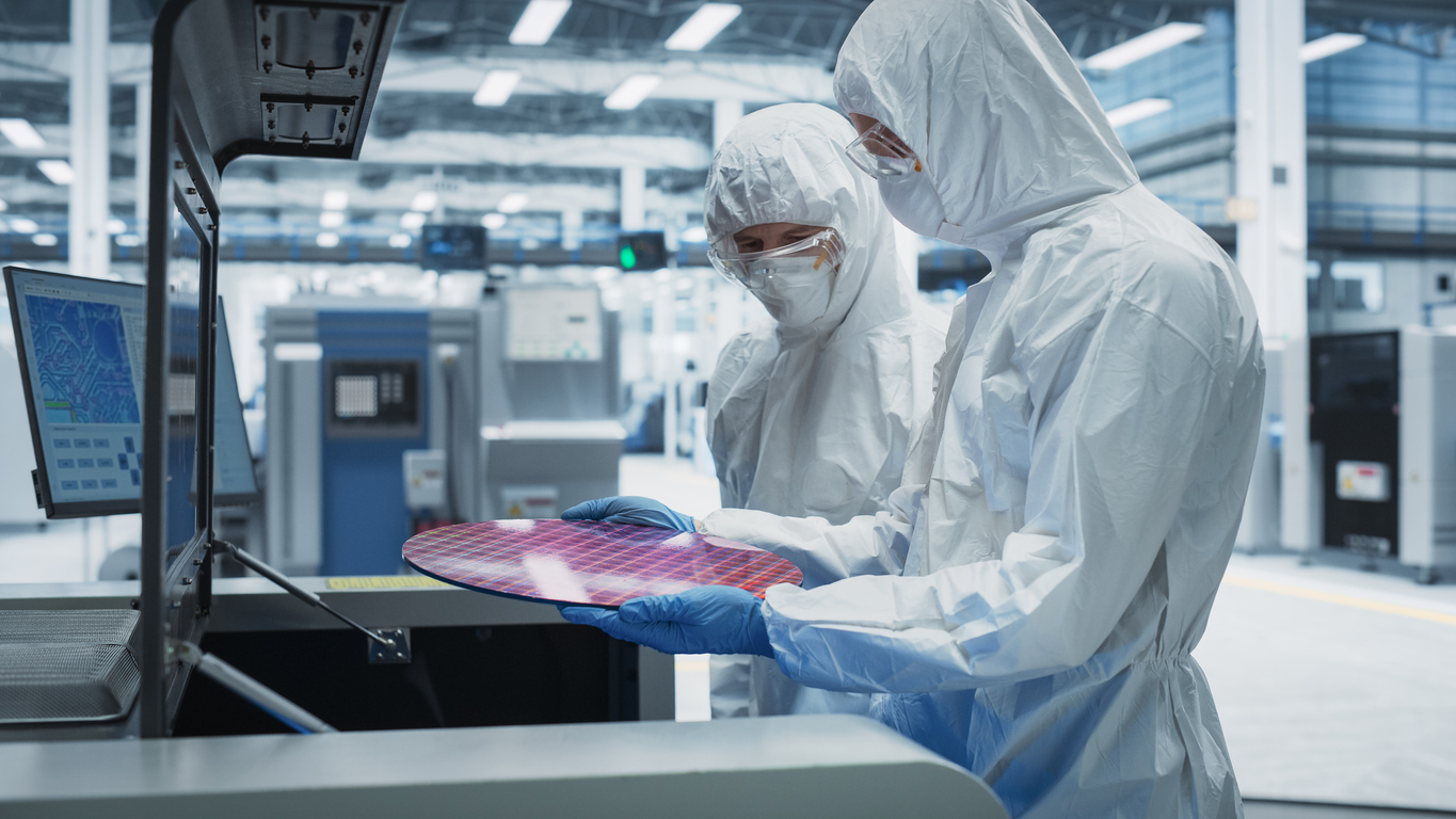
Two researchers examine a silicon wafer in a lab. iStock
Earlier this month, the Department of Commerce announced that Arizona State University will host the third and final flagship research and development (R&D) facility as part of the National Semiconductor Technology Center (NSTC) – a public-private consortium dedicated to accelerating innovations in semiconductor technology. The facility is being funded by the CHIPS and Science Act, which Congress passed in 2022 to bolster the American semiconductor supply chain through research and manufacturing and to reduce the nation’s dependence on China for microchips.
According to the Commerce Department, the R&D facility at ASU “will feature cutting-edge capabilities to bridge the gap between laboratory research and full-scale semiconductor production.” Specifically, the facility will “enable researchers and industry leaders to develop and test new materials, devices, and advanced packaging solutions in a state-of-the-art R&D environment.”
Packaging, in the context of semiconductor production, refers to materials that house microchips in order to protect them from heat and to allow for an efficient flow of electric current through them. “Advanced packaging,” according to ASU, is a critical part of the semiconductor design and manufacturing process that makes ever-smaller and more powerful chips “work faster and even combine[s] different kinds of chips onto one wafer for super advanced capabilities like artificial intelligence.” As the university explains, “It’s as if you had a glove that not only protected your hand but also made it stronger.”
ASU is a recognized leader in semiconductor research and known for “teaching advanced packaging to its students, creating the skilled workforce that’s desperately needed by the semiconductor industry.” The university has also partnered with private industry to expand research and development in advanced packaging.
The R&D facility will be located at ASU Research Park in Tempe, Arizona, and is expected to become operational by 2028. It is the third of three CHIPS for America R&D facilities; the other two facilities are the Design and Collaboration Facility in Sunnyvale, California, and the Extreme Ultraviolet Accelerator in Albany, New York.
“The CHIPS R&D project will create a national lab that will be the final piece in a semiconductor supply chain that serves the nation with research and development, manufacturing and workforce development all right here in Arizona,” said ASU President Michael Crow, continuing: “You’ll have all three things together in the same place to help the nation; Arizona will be the hub nationally – and ASU is at the center of the hub.”
Kritika Agarwal is senior editorial officer at AAU.